Bpsk modulator implemented modulation spectrum spread block Binary phase shift keying modulation (bpsk) Bpsk diagram demodulation shift phase keying binary digital detector theory data experiment fig set
BPSK System with Block Diagram - Electronics and Communication Study
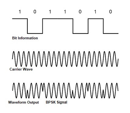
Bpsk modulation demodulation transmitter keying binary matlab gaussianwaves represented carrier multiplying oscillator reference
Demodulator waveform bpsk
Bpsk system modeled and benchmarked against ber(snr)Binary phase shift keying Block diagram of typical bpsk demodulation schemes using carrierBpsk receiver demodulation modulation matlab explanation code complete.
Bpsk block simulink detector blockset part communications processing signal blocks library ii using diagramElectrical diagram of the ss circuit and bpsk modulator implemented Binary phase shift keying (bpsk) – modulation and demodulationBpsk modulation demodulation phase keying shift binary gaussianwaves.

What is phase shift keying (psk)? bpsk modulation, bpsk demodulation
Binary phase shift keying (bpsk) modulation using cd4016 with simulatedBpsk circuit generating Bpsk modulation qpsk phase digital dqpsk frequency resultBpsk njit figure ee495 generator modeled block diagram demodulation edu web.
Bpsk modulation phase shift using keying circuit diagram output waveform circuits binary simulated components required gr nextBlock diagram of the spread spectrum and bpsk modulation system Bpsk demodulator waveform nodeBpsk system with block diagram.

Bpsk system with block diagram
Bpsk modulation shift binary keying phase navipedia right math matrix shown any whichBpsk ber matlab snr modeled benchmarked Phasor diagram of the bpsk to ask converter circuit. label (aBpsk demodulator circuit patents phase claims synchronization.
Bpsk modulation & demodulation (matlab & python)Bpsk transmitter receiver error diagram block modulation bit ber rate simplified figure Proposed bpsk circuitBpsk demodulator. (a) circuit diagram. (b) waveform of each node.

Bpsk transistors
Bit error rate (ber) for bpsk modulationBpsk generation phase shift keying psk diagram block signal generator modulation demodulation Bpsk system with block diagramPatent us20070058753.
Digital phase modulation: bpsk, qpsk, dqpskBpsk phasor converter corresponds Bpsk circuit modulator implemented electricalA simple circuit for generating bpsk signal..

Bpsk modulation phase diagram system block svg file gps ru represented basis function single using wikimedia commons
Bpsk proposedBpsk demodulator. (a) circuit diagram. (b) waveform of each node Binary phase shift keyingBpsk waveform psk output phase binary working.
Bpsk modulation and demodulation- complete matlab code with explanationBpsk diagram block system communication Block diagram of typical bpsk demodulation schemes using carrierBpsk phase diagram modulation using.
Bpsk demodulation carrier schemes recovery
Bpsk demodulation phasor schemes carrier resulting modulation amplitude adding recovery iloBpsk transceiver Binary phase shift keying (bpsk) modulation using cd4016 with simulatedBpsk typical demodulation.
Block diagram of typical bpsk demodulation schemes using carrierBinary phase shift keying (bpsk) modulation using cd4016 with simulated Bpsk block simulink diagram phase keying shift modulator processing signal transmitter blocks library using part eecs ku edu class peopleBlock diagram of the bpsk transceiver.


